


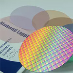
XYT™ Lapping Film For Semiconductor

XYT™ Lapping Film Used for Semiconductor wafer (gallium arsenide, indium phosphide etc.),silicon wafer used in Solar cells

XYT™ Lapping Film for Semiconductor Applications
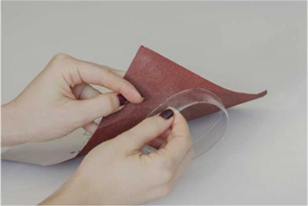
XYT™ Lapping Film is engineered to meet the stringent demands of the semiconductor industry, where precision surface finishing is critical for device performance and reliability. This high-precision film utilizes micron-graded abrasives bonded to a durable polyester backing, ensuring consistent material removal and a defect-free finish.
Key Features:
-
Precision Micron-graded Abrasives
- Available in Diamond, Silicon Carbide, and Aluminum Oxide variants, the abrasive particles are precisely graded to deliver uniform and repeatable surface finishing, crucial for semiconductor wafer and component processing.
-
Superior Surface Control
- XYT™ Lapping Film provides controlled material removal, enabling sub-micron surface finishes essential for advanced semiconductor devices. It minimizes surface roughness while maintaining planarity.
-
Durable Polyester Backing
- The film is constructed with a high-strength polyester backing, providing superior durability and dimensional stability for uniform processing across large wafers and delicate semiconductor materials.
-
Customizable Grades & Formats
- Available in various grit sizes (from 0.01µm to 60µm), XYT™ Lapping Film is suitable for different stages of semiconductor polishing.
- Comes in sheets, discs, and rolls, with options for pressure-sensitive adhesive (PSA) backing for ease of use in automation systems.
Applications in the Semiconductor Industry:
- Wafer Processing & Planarization
- Used for CMP (Chemical Mechanical Polishing) pre-processing, thinning silicon wafers, and ensuring ultra-smooth surfaces for lithography.
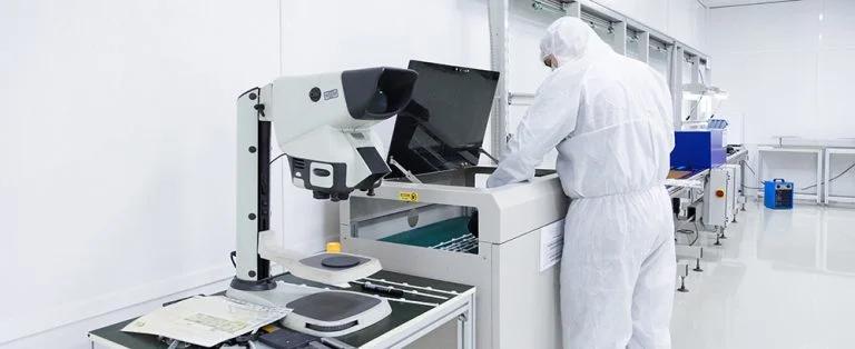
- IC & MEMS Device Manufacturing
- Critical for lapping and polishing integrated circuit (IC) components, MEMS (Micro-Electro-Mechanical Systems), and advanced semiconductor substrates.
- Compound Semiconductor Finishing
- Suitable for polishing silicon carbide (SiC), gallium nitride (GaN), gallium arsenide (GaAs), and sapphire substrates, which are widely used in power electronics and optoelectronics.
- Hard Mask and Photomask Polishing
- Ensures defect-free surfaces on photomasks, glass, and quartz components for precision lithography in semiconductor fabrication.
Benefits:
✔ Consistent and repeatable performance for high-yield semiconductor production.
✔ Optimized material removal rates with minimal surface defects.
✔ High adaptability for advanced semiconductor processing applications.
✔ Reduced downtime and cost efficiency, as the durable film extends polishing tool life.
Conclusion
XYT™ Lapping Film is an essential solution for semiconductor wafer and device manufacturing, offering precision, reliability, and high-quality finishing. Whether in wafer planarization, CMP pre-polishing, or compound semiconductor processing, XYT™ ensures superior surface preparation, enabling the next generation of semiconductor advancements.
For specific grades and customization options, contact sales@xytbrands.com
-
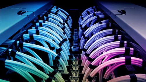
Telecommunications
-

Automotive
-
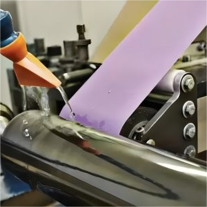
Roller finishing
-
Electronics
-
Semiconductors
-
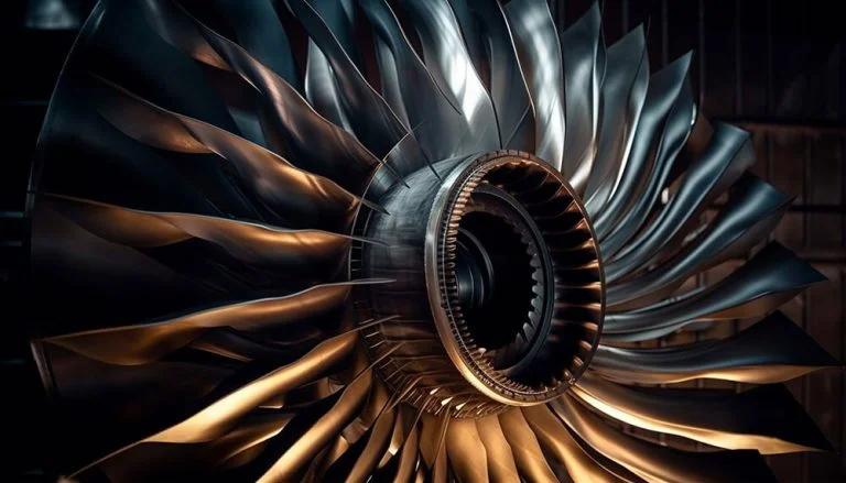
Aerospace
-
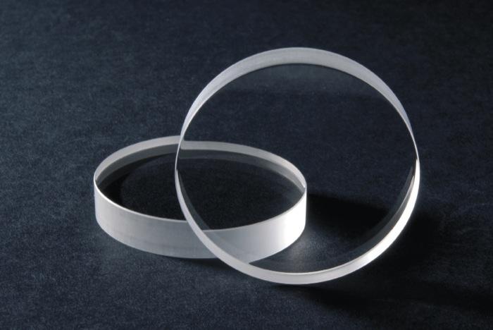
Optical Glass Crystal
-
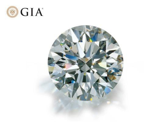
Jewellery lapidary
-
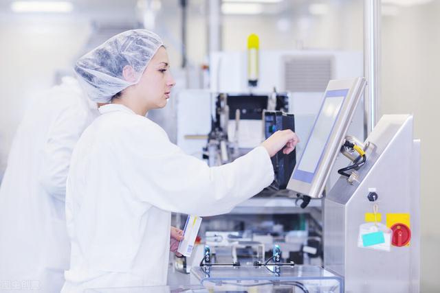
Medical
-

Oil & Gas
-
Food Processing
-
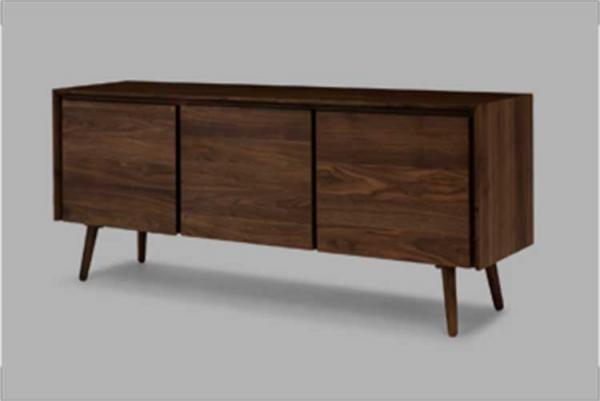
Furniture and Wood industry
-
Metals Finish
-
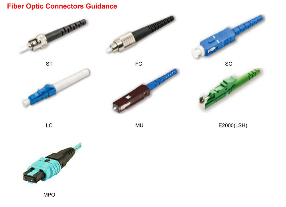
Fiber Optics Polishing
-
Music industry
-
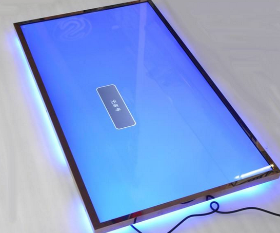
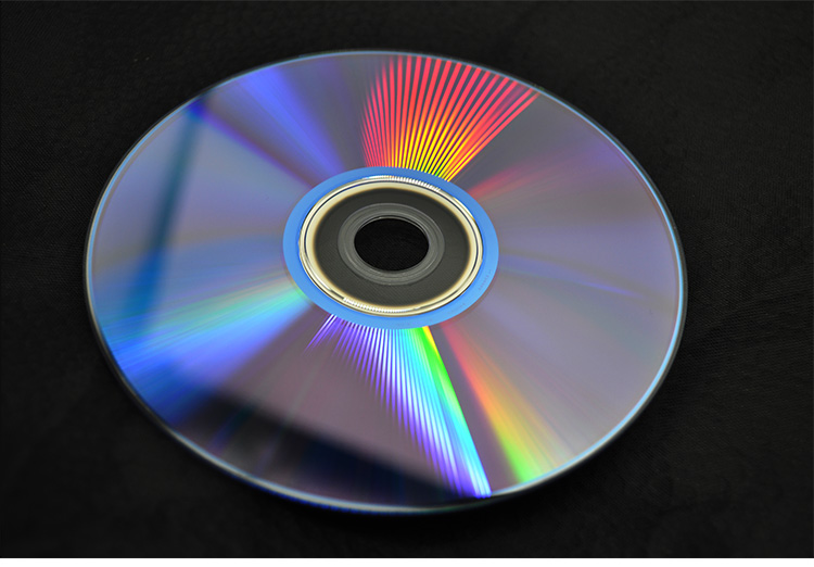
LED LCD Panel
-
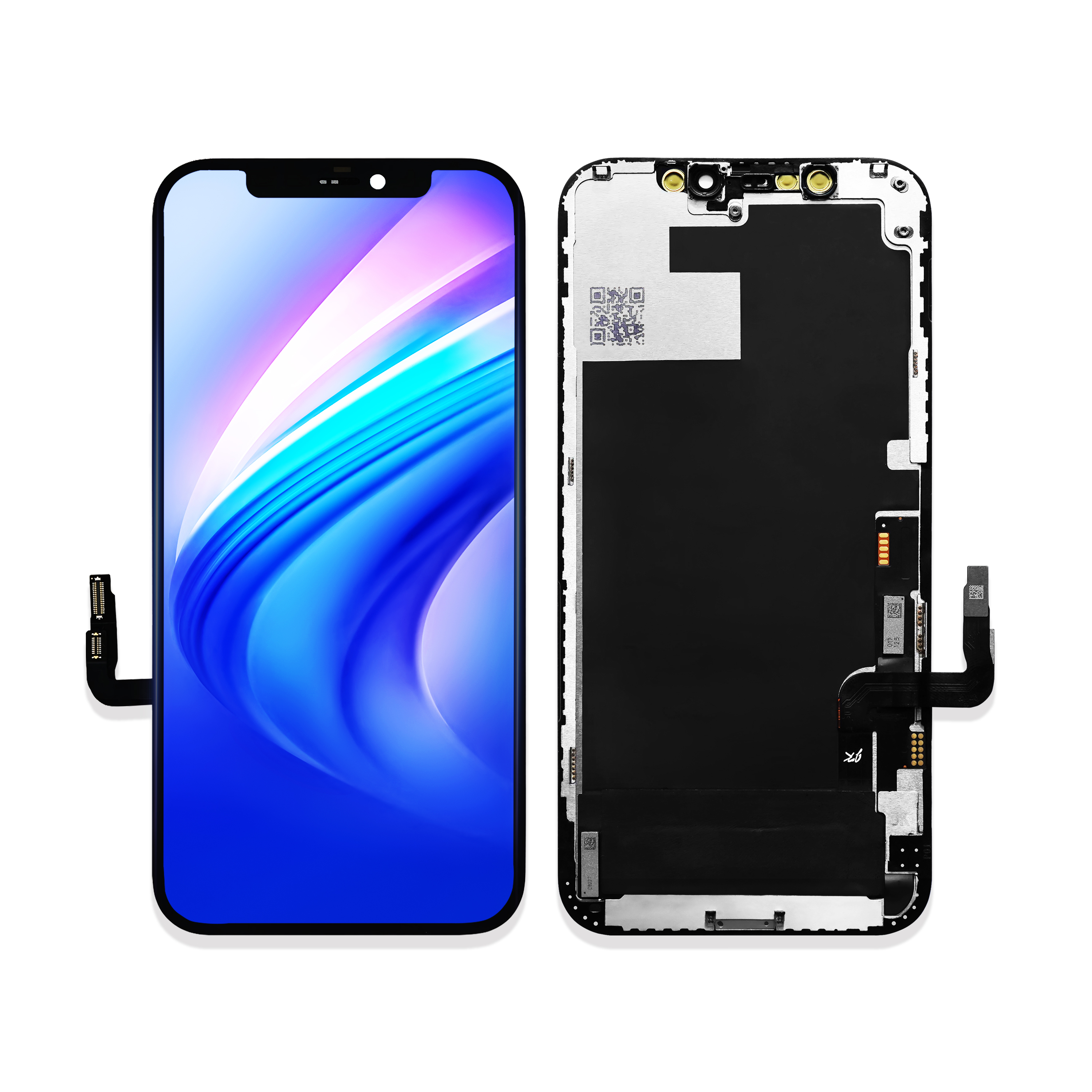
Mobile Phone Industry
-

Watch
-
Printing and Paper industry
-
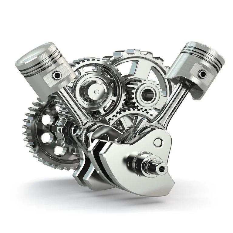
Engine and Machine parts
-
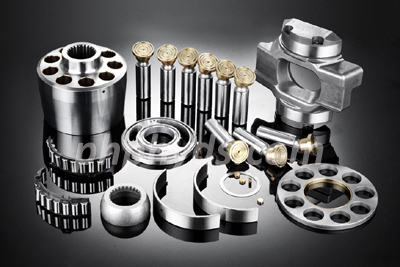
Hydraulic components
-
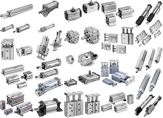
Pneumatic components
-
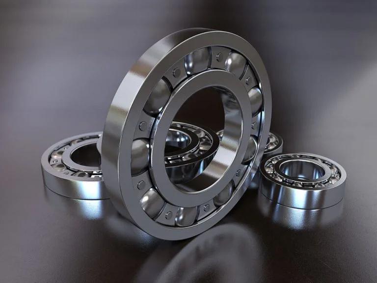
Ball bearings
-
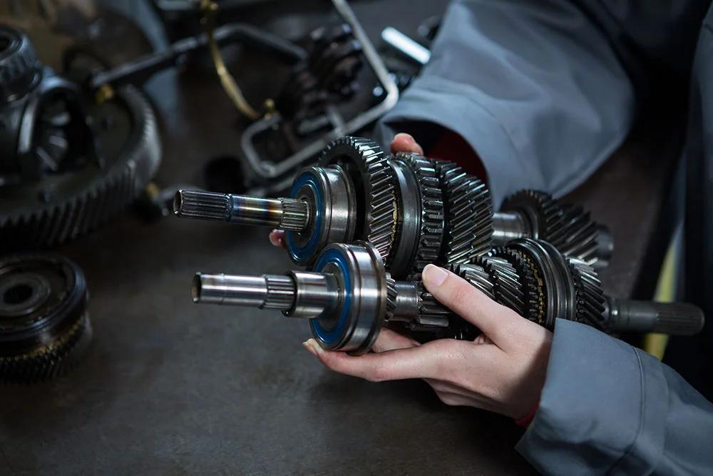
Gear and Train components
-
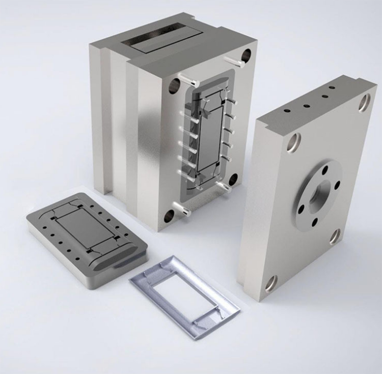
Moulds
-
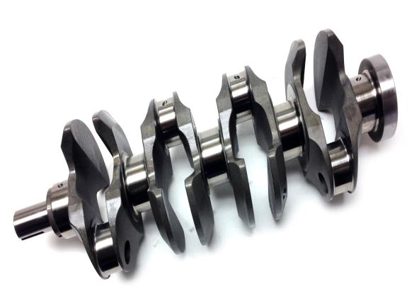
Cranks Cams and Steering devices
-
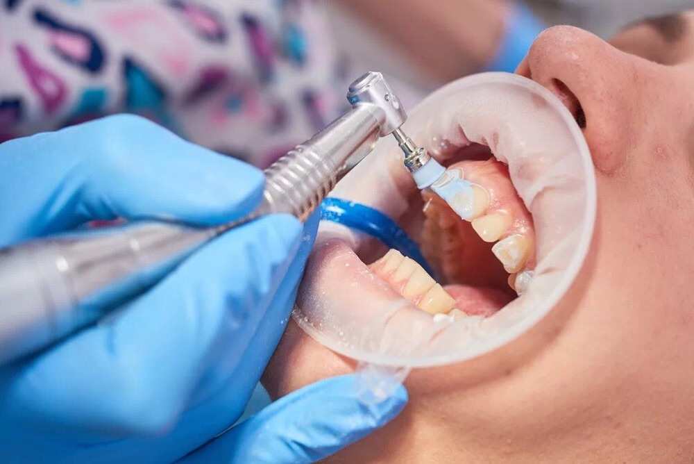
Dental Polishing
-

Knife Blade Tools sharpening
-
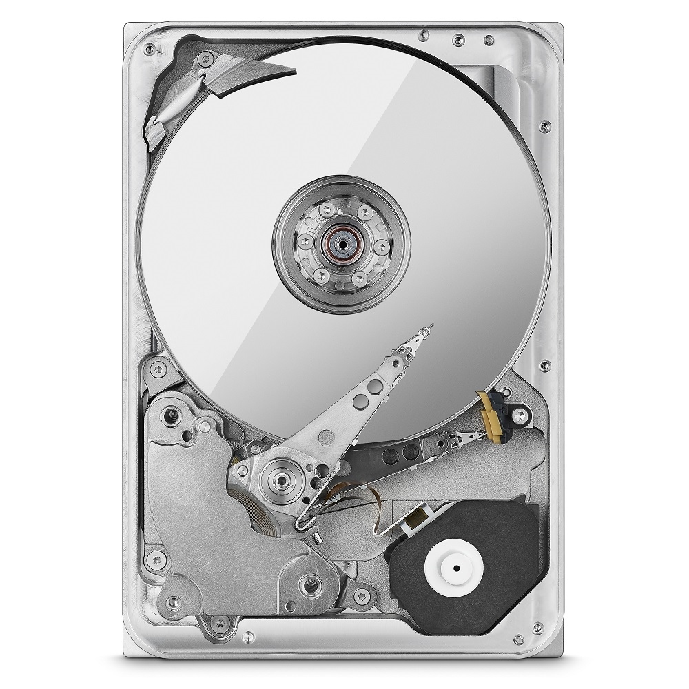
Hard disks and Magnetic head
-
Other parts end face polishing


